- Home
- Learn Linux
- Learn Electronics
- Raspberry Pi
- Programming
- Projects
- LPI certification
- News & Reviews

Google Ads
I have already explained how you can use an off-the-shelf pre-built Arduino or compatible board.I have also covered how to design an Raspberry Pi HAT in Fritzing. Fritzing is a useful program for beginners, but there are more professional tools that can be used to create professional circuits. KiCAD is one such tool, which is available as Free Open Source software. It takes a bit more work to get familiar with it, but you will see that it is a very powerful tool without some of the limitations of the free options of commercial software.
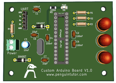
Here I'm going to show how you can create your own custom Arduino like circuit as a PCB using KiCAD. This is based around the ATMega ATMEL microcontroller ATmega328p.
In part one I show how to create the schematic diagram. This uses the ATmega328p and some basic components such as a crystal, capacitor, resistors and LEDs. I've also added some diodes to protect against incorrect polarity and connectors for the power and uarts. The circuit mainly uses through hole technology (THT) components, but also includes some optional SMD mounted components.
After designing the circuit the next stage is to design a printed circuit board. The Pcbnew tool in KiCAD is used to lay out the components and tracks to create a complete PCB design which can be plotted to gerber files ready for professional fabrication.
The PCB is created by first associating each of the components with their respective footprint, arranging them around the board and then laying the tracks based on the ratsnest wires from the schematic diagram.
Once the design is complete then it can be sent for fabrication.
To make a Printed Circuit Boards look more professional you can add text, images and logos. In this video I have shown how you can add small logos and large images to the front and back silk screen layers.
The technique above does not require any external applications other than what you use to create the image in the first place. It uses the standard bitmap to component converter to take a bitmap image and safe it as a component footprint file. This can be saved into a component library (.pretty directory) to be accessible from Pcbnew.
The components can then be soldered onto the PCB. The SMD components are optional, but it should be possible to solder those using either hand soldering or hot air based reflow techniques. The rest of the components should be soldered by hand.
Components required
Note: Please check the sizes of the components against the PCB design.
Whilst I don't intend to use this as a production PCB for sale that would often be the aim in making custom PCBS. It is normally a good idea to manufacture a few boards first and to see if it works correctly and whether there are any improvements that could be made. Based on this prototype then you can decide on whether any changes are neccessary.
Some of the things I have considered that could be done differently.
I did not include any markings on the silk layer for which side of the screw terminal is positive which I did include in my other design.
The 1N4007 diodes do work, but if using a 5V power supply they do reduce the voltage down to be just below the recommended power for the ATmega328p running at 16Mhz. These may be better replaced with a 1N5817 or similar schottky diode which have a lower voltage drop. Alternatively if you are confident that you will not connect the power and UART at the same time then they could be replaced with jumper wire.
The other thing is that this would be better with the ability to control multiple traffic lights and perhaps with an I2C interface to allow control by a computer. These are both features that I included in the original design G-scale model railway traffic light project with custom electronics circuit and PCB. They were dropped from this version to shorten the video and make it easier to follow.
Below are the source files for the KiCad design, the gerber files used for production of the complete PCB and the Arduino code.
I'll be adding new projects based around my own custom circuits in future.
To be notified about future videos
Subscribe to the PenguinTutor YouTube Channel
Please view the copyright information regarding use of the circuits.

